- 您现在的位置:买卖IC网 > Sheet目录490 > NTLUS3192PZTBG (ON Semiconductor)MOSFET P-CH 20V 3.4A SGL 6UDFN
NTLUS3192PZ
Advance Information
Power MOSFET
? 20 V, ? 4.2 A, m Cool t Single P ? Channel,
ESD, 1.6x1.6x0.55 mm UDFN Package
Features
? UDFN Package with Exposed Drain Pads for Excellent Thermal
Conduction
? Low Profile UDFN 1.6 x 1.6 x 0.55 mm for Board Space Saving
? Lowest RDS(on) in 1.6x1.6 Package
? ESD Protected
? This is a Halide Free Device
? This is a Pb ? Free Device
Applications
? High Side Load Switch
? PA Switch and Battery Switch
? Optimized for Power Management Applications for Portable
Products, such as Cell Phones, PMP, DSC, GPS, and others
MAXIMUM RATINGS (T J = 25 ° C unless otherwise stated)
V (BR)DSS
? 20 V
http://onsemi.com
MOSFET
R DS(on) MAX
85 m W @ ? 4.5 V
115 m W @ ? 2.5 V
160 m W @ ? 1.8 V
250 m W @ ? 1.5 V
S
G
I D MAX
? 3.0 A
? 1.5 A
? 0.5 A
? 0.2 A
Parameter
Drain-to-Source Voltage
Symbol
V DSS
Value
? 20
Units
V
Gate-to-Source Voltage
V GS
± 8.0
V
D
1
m COOL t
Continuous Drain
Current (Note 1)
Power Dissipation
(Note 1)
Continuous Drain
Current (Note 2)
Steady
State
t ≤ 5s
Steady
State
t ≤ 5s
Steady
State
T A = 25 ° C
T A = 85 ° C
T A = 25 ° C
T A = 25 ° C
T A = 25 ° C
T A = 25 ° C
T A = 85 ° C
I D
P D
I D
? 3.4
? 2.4
? 4.2
1.5
2.3
? 2.2
? 1.6
A
W
A
1
6
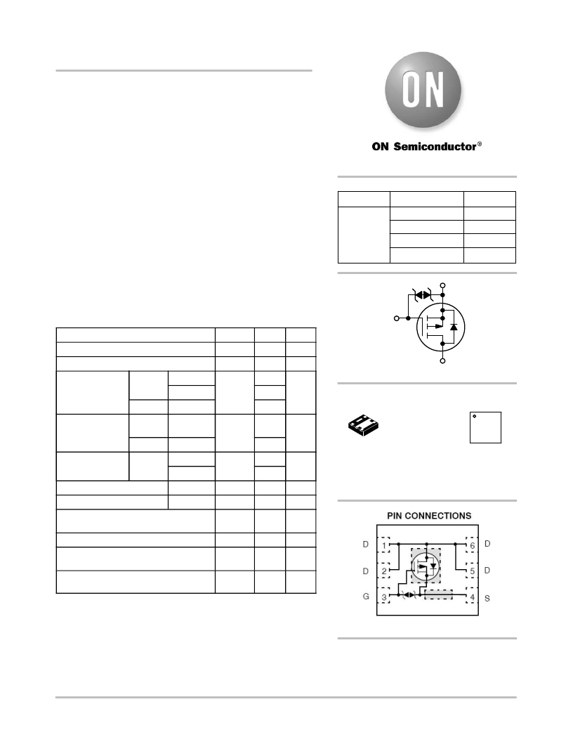
P ? Channel MOSFET
MARKING
DIAGRAM
UDFN6
CASE 517AU AA M G
G
AA = Specific Device Code
M = Date Code
G = Pb ? Free Package
Power Dissipation (Note 2)
Pulsed Drain Current
T A = 25 ° C
tp = 10 m s
P D
I DM
0.6
? 17
W
A
(Note: Microdot may be in either location)
Operating Junction and Storage
Temperature
Source Current (Body Diode) (Note 2)
Lead Temperature for Soldering Purposes
(1/8 ″ from case for 10 s)
Gate-to-Source ESD Rating
(HBM) per JESD22 ? A114F
T J ,
T STG
I S
T L
ESD
-55 to
150
? 1.0
260
1000
° C
A
° C
V
Stresses exceeding Maximum Ratings may damage the device. Maximum
Ratings are stress ratings only. Functional operation above the Recommended
Operating Conditions is not implied. Extended exposure to stresses above the
Recommended Operating Conditions may affect device reliability.
1. Surface Mounted on FR4 Board using 1 in sq pad size (Cu area = 1.127 in sq
[2 oz] including traces).
2. Surface-mounted on FR4 board using the minimum recommended pad size
of 30 mm 2 , 2 oz. Cu.
This document contains information on a new product. Specifications and information
herein are subject to change without notice.
(Top View)
ORDERING INFORMATION
See detailed ordering and shipping information in the package
dimensions section on page 5 of this data sheet.
? Semiconductor Components Industries, LLC, 2009
May, 2009 ? Rev. P3
1
Publication Order Number:
NTLUS3192PZ/D
发布紧急采购,3分钟左右您将得到回复。
相关PDF资料
NTLUS3A18PZTBG
MOSFET P-CH 20V 8.2A 6UDFN
NTLUS3A39PZTBG
MOSFET P-CH 20V 5.2A 6UDFN
NTLUS3A40PZTBG
T4 20/8 PCH 2X2 UDFN SING
NTLUS3A90PZTBG
POWER MOSFET 20V 3A 60 MO UDFN6
NTLUS4195PZTBG
MOSFET P-CH 30V 3A SGL 6UDFN
NTMD2C02R2SG
MOSFET N/P-CH COMPL 20V 8-SOIC
NTMD2P01R2G
MOSFET PWR P-CHAN DUAL 16V 8SOIC
NTMD4184PFR2G
MOSFET P-CH 30V 2.3A 8-SOIC
相关代理商/技术参数
NTLUS3A18PZ
制造商:ONSEMI 制造商全称:ON Semiconductor 功能描述:a??20 V, a??8.2 A, Single Pa??Channel, 2.0x2.0x0.55 mm Cool UDFN Package
NTLUS3A18PZCTAG
制造商:ON Semiconductor 功能描述:PFET UDFN 20V 8.2A 18MOHM - Tape and Reel 制造商:ON Semiconductor 功能描述:REEL / PFET UDFN 20V 8.2A 18MOHM
NTLUS3A18PZCTBG
制造商:ON Semiconductor 功能描述:PFET UDFN 20V 8.2A 18MOHM - Tape and Reel 制造商:ON Semiconductor 功能描述:REEL / PFET UDFN 20V 8.2A 18MOHM
NTLUS3A18PZTAG
功能描述:MOSFET T4S PCH 20/8V IN 2X2 UDFN
RoHS:否 制造商:STMicroelectronics 晶体管极性:N-Channel 汲极/源极击穿电压:650 V 闸/源击穿电压:25 V 漏极连续电流:130 A 电阻汲极/源极 RDS(导通):0.014 Ohms 配置:Single 最大工作温度: 安装风格:Through Hole 封装 / 箱体:Max247 封装:Tube
NTLUS3A18PZTBG
功能描述:MOSFET T4S PCH 20/8V IN 2X2 UDFN
RoHS:否 制造商:STMicroelectronics 晶体管极性:N-Channel 汲极/源极击穿电压:650 V 闸/源击穿电压:25 V 漏极连续电流:130 A 电阻汲极/源极 RDS(导通):0.014 Ohms 配置:Single 最大工作温度: 安装风格:Through Hole 封装 / 箱体:Max247 封装:Tube
NTLUS3A18PZTCG
制造商:ON Semiconductor 功能描述:PFET UDFN 20V 8.2A 18MOHM - Tape and Reel 制造商:ON Semiconductor 功能描述:REEL / PFET UDFN 20V 8.2A 18MOHM
NTLUS3A39PZ
制造商:ONSEMI 制造商全称:ON Semiconductor 功能描述:a??20 V, a??5.2 A, Single Pa??Channel, ESD, 1.6x1.6x0.55 mm UDFN Cool Package
NTLUS3A39PZTAG
功能描述:MOSFET T4S PCH 20/8V IN 1.6X1.6
RoHS:否 制造商:STMicroelectronics 晶体管极性:N-Channel 汲极/源极击穿电压:650 V 闸/源击穿电压:25 V 漏极连续电流:130 A 电阻汲极/源极 RDS(导通):0.014 Ohms 配置:Single 最大工作温度: 安装风格:Through Hole 封装 / 箱体:Max247 封装:Tube
